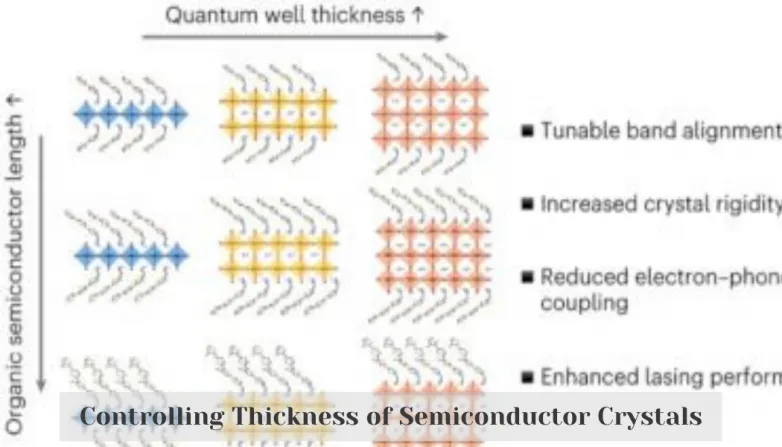
Controlling Thickness of Semiconductor Crystals
Sep 4, 2023 02:19 PM ET
- This research from Duke, Purdue, Yale, Lawrence Berkeley, CAS, Westlake and Huazhong Universities introduces a new technique to control the thickness of perovskite single crystals, which allows for tuning of electron and hole energy levels. The study's experimental and theoretical teams worked together to synthesize and characterize the materials and simulate their structure and properties. Led by Letian Dou and Volker Blum.

Researchers from Duke University, Purdue University, Yale University, Lawrence Berkeley National Laboratory, Chinese Academy of Sciences (CAS), Westlake University and Huazhong University of Science and Technology have developed a technique to control the thickness of phase-pure organic semiconductor-incorporated perovskite single crystals. This method allows for the tuning of electron and hole energy levels, affecting the materials’ optoelectronic properties and capacity to emit light. The experimental and theoretical teams collaborated to synthesize and characterize the materials, and computationally simulate their structures and properties. The study was led by Letian Dou and Volker Blum.
How Was the Thickness of Organic Semiconductor-Incorporated Perovskite Single Crystals Controlled?
- The team used a ‘halide exchange’ approach to control the thickness of organic semiconductor-incorporated perovskite single crystals.
- The halide exchange process involves exchanging anions, such as iodide, chloride and bromide, in a perovskite crystal matrix with an organic anion.
- This process allows for the formation of different size crystals with different thicknesses, ranging from 0.7 nanometers to 6.8 nanometers.
- The team then characterized the optical and electronic properties of the materials, examining their optoelectronic properties and capacity to emit light.
- The team found that the thickness of the crystals had a significant impact on the materials’ properties, affecting their optoelectronic properties and capacity to emit light.
- The study has implications for the development of organic semiconductor-based optoelectronic devices, which could be used for applications such as energy harvesting, light emitting devices, displays and photovoltaics.
Also read

