Renesas Electronics Releases the First Bidirectional 650V-Class, D-Mode GaN Switch for Solar Microinverters
Tokyo-based advanced semiconductor manufacturer, Renesas Electronics, has recently introduced the industry’s first bi-directional switch that uses depletion-mode (d-mode) GaN technology, which is capable of blocking both positive and negative currents in a single device with DC blocking. Given the part number TP65B110HRU, this GaN switch simplifies power converter designs significantly while also replacing back-to-back FET switches with a single device that is easy to drive and switches quickly while experiencing low power losses. The device is also capable of providing soft and hard switches with quick and clean transitions between on and off, and is also compatible with standard gate drivers. This performance targets single-stage solar microinverters, as well as onboard EV chargers, and AI data centers.
Renesas TP65B110HRU vs. Other High-Power Conversion Designs
Modern high-power conversion designs currently rely on Silicon Carbide (SiC) or unidirectional silicon, both of which block current in one direction in their “off” states. This means they can’t handle all the power conversion by themselves, so this process must be split into multiple stages that are handled using different switched bridge circuits. Solar microinverters, for instance, have a full bridge (four switch) circuit to handle DC to AC conversion in the first stage, which is followed by a second stage that produces the final AC output that can be injected into the grid. This forms a 2-stage system.
There have been attempts to make efficient single-stage DC-to-AC converters, but these end up using back-to-back conventional unidirectional switches, which increase the switch count 4X, resulting in lower efficiency figures.
Renesas’ TP65B110HRU GaN switch changes this efficiency conversation entirely because it integrates both positive and negative current blocking in a single device. This means DC-to-AC power conversion in a microinverter can now be done using an efficient single-stage process that requires fewer devices, which in this case are only two high-voltage SuperGaN bidirectional switches. So the circuit only needs half the switch bridge count (two instead of four), and there’s no need for DC-link capacitors in between. On top of that, these GaN switches flip quickly with low stored charge in between, which allows them to switch at higher frequencies and with higher power densities and low capacitance than their SiC and unidirectional silicon counterparts.
In actual figures, these GaN switches have demonstrated more than 97.5% power efficiency in a single-stage microinverter setup, which is as a result of the fast switching capability and zero back-to-back connections. This improvement is critical in solar installations because it cuts energy conversion losses, leaving more power to flow into the grid or retaining more energy in the battery to last though the night, especially in seasons where there’s less daylight.
Key Features of the TP65B110HRU 650V-Class GaN Switch
-
+/-650V continuous peak AC and DC rating (+/-800V transient rating)
-
2kV Human Body Model ESD protection rating (HBM and CDM)
-
3V typical Vgs(th)
-
110 mΩ typical RSS,ON @ 25⁰C
-
Zero negative drive required
-
±20V maximum Vgs
-
>100 V/ns dv/dt immunity
-
1.8V, VSS,FW freewheeling diode voltage-drop
-
TOLT top-side cooled package with industry standard pin-out
This GaN chip is based on a proprietary normally-off technology, and its physical design comprises a high-voltage bidirectional d-mode GaN switch that is co-packaged with two low-voltage silicon MOSFETs with a high 3V threshold voltage, and a high +/-20V gate margin. It also features built-in body diodes to provide efficient reverse conduction.
Since this chip uses depletion mode, it is compatible with standard gate drivers that need no negative bias (enhancement-mode bidirectional GaN switches aren’t compatible with standard gate drivers). This compatibility results in a lower-cost and simpler gate loop design that provides quick and stable switching in both hard and soft switching operations without any negative impact on performance and efficiency.
So hard switching power conversion topologies, such as the Vienna-style rectifier, can utilize the switch’s high dv/dt capability of over 100V/ns with short delays during the on/off switching and minimum ringing.
Besides performance, this field-proven SuperGaN switch simplifies inverter designs by reducing the required PCB real estate, cutting the overall system cost, and accelerating the design time because Renesas provides system-level integration with power management chips, controllers, and gate drivers.
TP65B110HRU GaN Switch Availability
The TP65B110HRU GaN chip switch is already available, and customers can purchase its evaluation kit (RTDACHB0000RS-MS-1) to test the IC with different drive options, implement ZVS soft switching, and detect AC zero crossings.
Since this chip is new, Renesas provides over 400 winning combinations with a wide variety of products from the Renesas lineup to enable customers to speed up their product design processes and bring these products to market as quickly as possible. These combinations consist of the 500-watt solar microinverter and hard-switching 3-phase Vienna rectifier system solutions, which combine the GaN switch with compatible Renesas devices. All of them are technically vetted system architectures from mutually compatible devices that operate seamlessly to bring about a low-risk, optimized design that helps to reduce the time to market for the final product.
Sample Winning Combination (Single-Stage Dual Active Bridge Solar Microinverter)
Since renewable energy is becoming quite popular, inverters are one of the most sought-after consumer products. This single-stage microinverter can deliver up to 500 watts using two GaN switches, and it features a primary DC to AC full bridge converter, a secondary AC to AC bridge using two Renesas GaN switches, and a high-frequency transformer. The secondary GaN switch bridge is responsible for providing quick, low-loss switching while maintaining a low total harmonic distortion of less than 3% for 50/60Hz on-grid and off-grid operations.
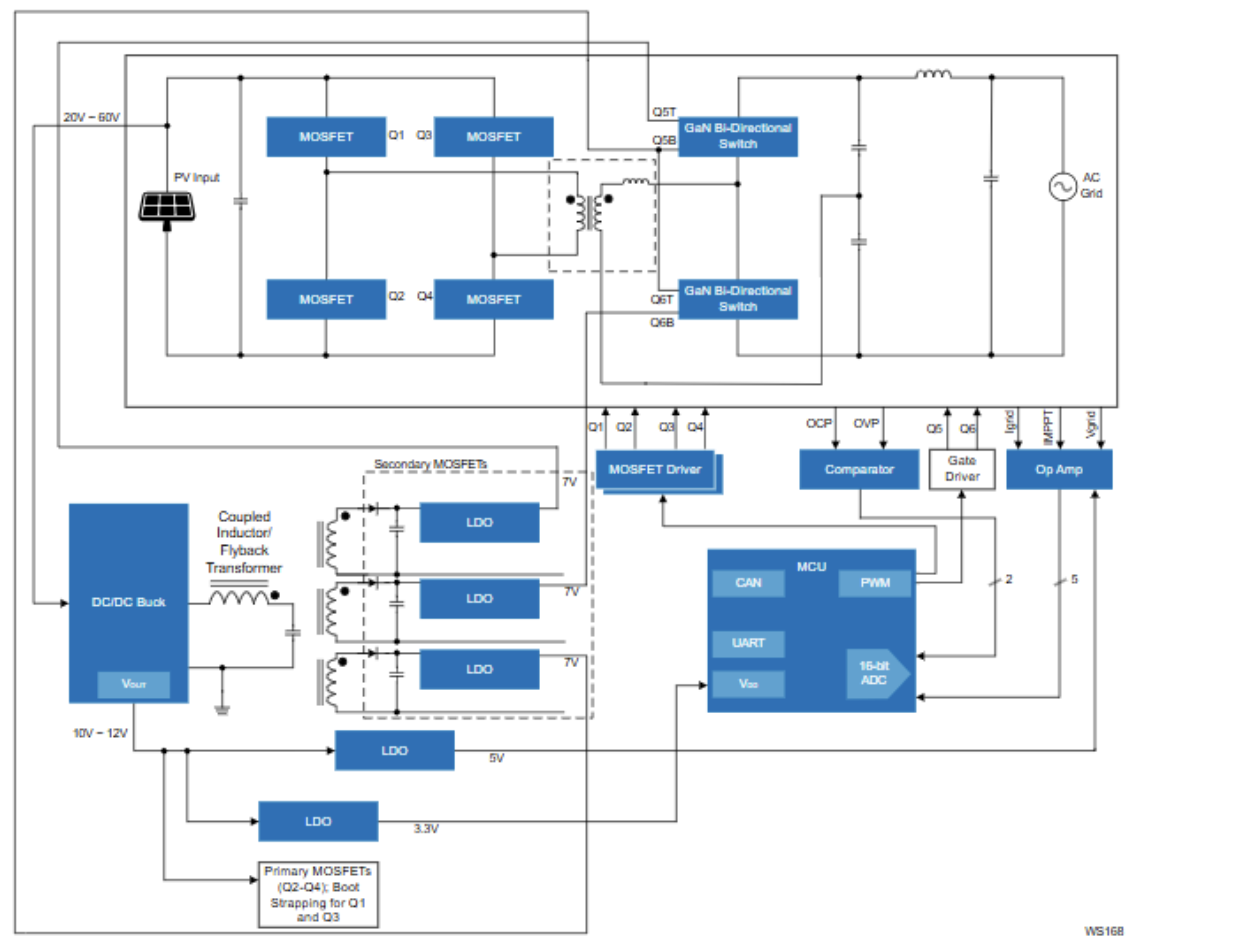
Img src: Renesas.com
This inverter features an Arm® Cortex® MCU to run the MPPT algorithms while providing power flow control and real-time monitoring. Conventional flyback-based microinverters are limited to delivering 250 watts and require multiple switching stages, which bring about more switching capacitances and on-state resistance. But this GaN bidirectional switch achieves a higher power output with fewer devices, better efficiency, a higher power density, and a smaller overall PCB design.
Also read
- Silicon Perovskite Tandem Solar Cell Molecular Additive To Boost Solar Cell Efficiency To 32.76%
- Researchers Discover “Spin Flip” in Metal Complexes That Push Solar Energy Conversion to 130%
- How Artificial Intelligence Enhances Hybrid Inverter Performance in Solar Systems
- Plug-In Solar Panels Are About To Explode and Here’s How To Tap Into This Market
- Adani Group Is Building One of the Largest Energy Storage System To Provide Reliable Grid Power