LONGi Hits 35.5% Certified Perovskite-Silicon Tandem Record
- LONGi claims a world-record 35.5% certified crystalline silicon–perovskite tandem efficiency—topping its prior 34.85% milestone—presented in Shanghai and verified by ESTI, signaling rapid R&D momentum.
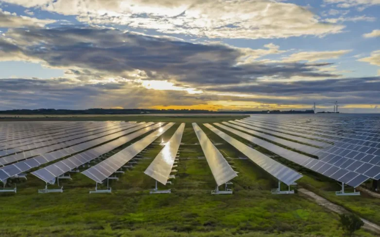
LONGi says it has set a world record for crystalline silicon–perovskite tandem solar cells, reporting a certified 35.5% power conversion efficiency. The result was presented July 14, 2026 at the company’s Solar and Storage Innovation Technology Conference at Shanghai Jiao Tong University and was certified by the European Solar Test Installation (ESTI).
The two-terminal device pairs a wide-bandgap perovskite top cell with a crystalline silicon bottom cell. LONGi did not disclose the active area or full electrical details, suggesting the figure reflects a laboratory-certified cell milestone rather than a commercial module. The company cited a prior 34.85% certified by NREL in April 2025 and framed the announcement within its “Technology Forest” R&D program, underscoring fast progress as tandem systems remain in research.
What does LONGi’s certified 35.5% silicon–perovskite tandem record mean?
- A “certified 35.5%” value means an independent testing organization verified the measured power-conversion efficiency of a specific tandem cell, rather than it being an internal or estimated result from simulations.
- The efficiency figure is “power conversion efficiency,” typically defined as the ratio of electrical power output to the incident solar power under standardized test conditions; in tandem devices it reflects how well both sub-cells convert sunlight into electricity across the spectrum.
- The record pertains to a two-terminal crystalline silicon–perovskite tandem architecture (top perovskite cell + bottom crystalline silicon cell) rather than separate single-junction devices, indicating progress in stacking complementary light absorption in one device.
- A silicon–perovskite tandem targets higher efficiencies than single-junction silicon by using a wide-bandgap perovskite top layer to capture higher-energy photons and a silicon bottom layer to capture lower-energy photons.
- “World record” language generally signals the highest certified efficiency figure among similar device types at the time of certification, with the certification process used to ensure comparability across labs.
- Certification by ESTI implies the measurement followed controlled procedures for factors that affect tandem performance—such as illumination spectrum, temperature, and calibration—so the result is more directly comparable to other certified records.
- Because tandem efficiency can be sensitive to device area, interconnection quality, and measurement setup, a certified record at the cell level usually represents a milestone for cell physics and fabrication quality, not automatically the performance of a mass-produced module.
- The published result indicates that long-standing bottlenecks in perovskite/silicon tandem research—such as maintaining perovskite stability and achieving efficient charge transfer between layers—are reaching commercially relevant performance ranges.
- The use of a crystalline silicon bottom cell also suggests compatibility with established silicon manufacturing knowledge, even if further engineering is still required to translate lab-certified performance into durable, large-area production.
- In the R&D context, a certified 35.5% benchmark serves as a reference point for the next stages of development: scaling active area, improving yield, and testing long-term stability under realistic operating conditions.
- Practically, this kind of record raises the ceiling for potential system-level economics: higher cell efficiency can reduce the amount of active material needed per watt, though actual cost and energy yield depend on module design, lifetime, and balance-of-system factors.